Suggested Reading: Horowitz and Hill pp. 470-491
Equipment
A. Digital to Binary Encoding

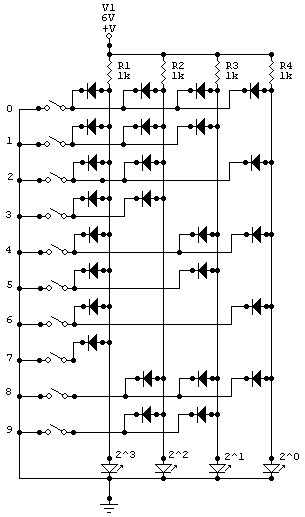
This could be a very basic building block of a computer, which needs to encode everything into binary. If you close the switch next to one of the decimal numbers, that number is displayed in binary by the LED's.
Build this circuit using standard diodes and LED's. You do not actually need the 10 switches, as you can just attach and detach a wire at those points (open circuit and closed circuit.) Note that where wires cross, there is no connection. Connections are only made at nodes (dots).
Be sure to understand the operation of this circuit. What happens when you close more than one switch at once? Imagine what you would have to do to encode the entire 256 ASCII character set every computer uses. Note that in the ASCII character set, the numbers 0-9 are not actually defined as their own value: they are encoded as decimal numbers 48-57. In character encoding, the colon follows 9, so in our scheme would be given the decimal value 10. If we wanted to add decimal value 10 to this circuit, what would that additional part of the circuit look like? (Either draw it into the circuit given, or describe in words what circuit element goes where.)
B. Logic Circuits - another building block
Caution, in all work with logic circuits:
1) Never apply > 5V or <0V to the digital circuits or to the Logic Probe and
Digital Pulser.
2) Never run TTL circuits from any supply other than +5V and GND.
Violating these rules results in certain destruction of various IC’s and equipment.
You can create the needed 5V and 0V signals in a number of ways:
Logic Probe and Digital Pulser
The LP and DP are very easy to use, but you must take precautions to hook them up correctly and to not give them voltages greater than 5V!
I will show you how to use the LP and DP, and in addition you can use the instruction manuals. Be sure they are set for the correct type of logic (TTL in this case).
B1: Discrete Component Gates
Diode Gates
Build the diode OR gate. Be sure you understand the operation of the LP and DP by using the DP as one of the inputs, and detecting the output with the LP. Power them with a 5V power supply. Try using both a single pulse and a continuous pulse input. Then try setting one of the inputs at a level 5V using the power supply, and detect the output with the LP.
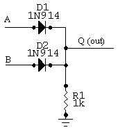
Diode OR gate.
Build the AND gate, below. Confirm that the AND and OR gates have the expected truth tables using either power supplies or the probes. What are the output voltage levels (both low and high, for both circuits); you can use a multimeter for this. Be sure you are using 0.0 V (GND) and 5.0 V as the low and high inputs. What is the fanout of any diode gate? (You do not need to set up any circuits for this last question.)
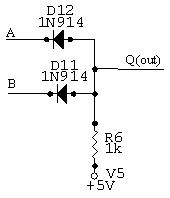
Diode AND gate.
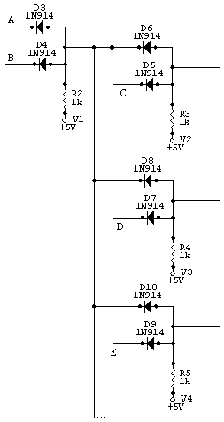
Fanout: is the number of gates that the output from a single gate can drive. (Note: above diagram is for illustration purpose, you do not need to build it.)
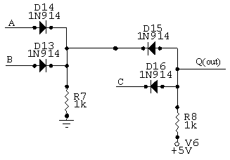
Cascaded OR and AND configuration.
Make all the same measurements for the series combination of the AND and OR as shown. What is the theoretical and measured truth table for this 3-Input gate? Is there a difference? Why couldn’t you build a large logic circuit entirely from diode gates?
Solution to the problem illustrated by the last question: Discrete TTL NAND gate.
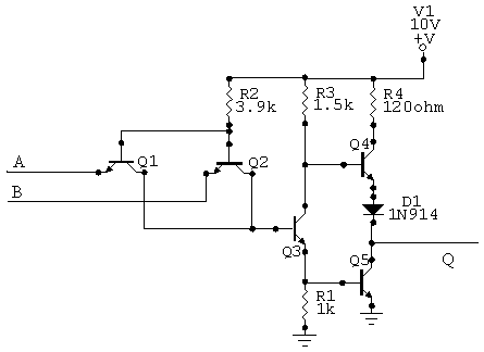
All transistors are 2N3904.
Construct the TTL NAND gate in Circuit Maker. Drive the inputs with level 0.0 or 5.0 V inputs, and verify that the output is a true NAND function of them. Measure the actual high and low output voltages. Try to explain how this circuit works (hint: the transistors are acting like switches, think about when each is open and closed).
B2: IC Gates
As always, with something useful and common, you can find an integrated circuit to do something that you used discrete components for. Here we will use IC gates to create the XOR function:
Exclusive OR
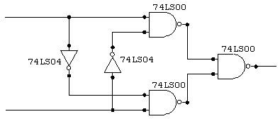
Exclusive OR.
Use logic (on paper) to show that this circuit performs the XOR function. Then construct it with TTL integrated circuits, 74LS00 (quad NAND) and 74LS04 (hex inverter), and try it out. Use the pinouts shown at the end of the lab (on the Web). If you get into the habit of pointing all the chips the same way on the breadboard, the power supplies become very easy to wire up.
B3: Multiplexer
Here we use more complicated digital logic, on an IC, to carry out a very useful function
Get a 74LS151 ‘8 input multiplexer’ IC and investigate its operation. Connect an LED indicator to its output Q (or Y) (use the pinout appendix), set up an address* on inputs A,B,C (or S0, S1, S2) and ground the STROBE (or ENABLE) input, ground each one of the data input lines D0 to D7 (I0-I7) (Note: an open TTL input is seen as logic high) Un-ground each input in turn until you find out which one of them is being transmitted to the output. Do this for several addresses until you understand the function.
(74LS151, click picture for pinouts) All pins except Vcc and GND are shown.
*The three-bit address refers to one of the eight outputs. If you ground all three, you are addressing 0; if you hold A high and ground B, C, you are addressing 1; A=C=0, B=1, addressing 2; etc. A is the LSB (least significant bit, or 1's place).
This is a kind of kooky use of a multiplexer. You do not have to do this part.
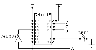
31-day machine. (74LS151) Pin connections other than Vcc and GND are labeled.
You can modify your circuit to construct the 31-day machine. This has a four digit input (A is the LSB) which is the binary number that represents the month. The circuit lights up the LED when the month whose number is applied to the input lines has 31 days in it!