Digital Circuits II: Basic Computer Operations
Objective: to learn about and
build on the basic building blocks of computers by introducing latches,
flip-flops, counters, and registers.
Suggested Reading: Horowitz and Hill pp. 504-515
Equipment:
- breadboard & jumper wires
- DC power supplies
- oscilloscope
-
push-button
switches
- in the Multisim virtual edition of this lab, these would be the "digital
pulser" or "digital constant":

- SPDT switch - use this where indicated even in a virtual simulation. Different types of switches were described in class.
- LEDs
- resistors
- 7400 - Quad NAND gate
- 74175 - Quad D Flip-Flop
1. Latches and
Flip-Flops: sometimes these two words are used interchangeably, but typically a
latch is sequential logic that is not
clocked (a bit of memory whose state is determined by the previous state and an
input), and a flip-flop refers to synchronous sequential logic (serves the same
purpose as a latch, but will only function when signaled by a clock.)
a) Connect
two NAND gates as shown in class to construct an SR latch. Connect SPDT
switches that you can switch between ground and 5V to the S and R inputs and LEDs to outputs Q and Q' (you need power
supply and grounds, too).

Note
b) Verify
that the "set" and "reset" inputs produce the expected
results.
c) Now set both inputs low. What are the outputs? Now try to switch both inputs simultaneously to high. What is the final state? Repeat this step several times. Do the outputs settle in the same state every time?
d) Is the truth-table for your SR latch as expected?
2. Debouncing
a switch:
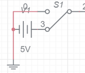
a) Observe the transition from on off state to an on state for a switch: Attach a SPDT switch to control the output of a 5V power supply, attach to a storage scope and capture the signal when the switch is activated (like the image in 1a, above). This is a different use of an oscilloscope than you are used to - we are not catching a repeated signal, but capturing something that only happens once. Do one of the appropriate parts below i, ii, or iii:
-
Using an Physical Oscilloscope: To capture a single event, see page 49 of the TDS-200 Series Oscilloscope User Manual or page 164 of the BK Precision scope manual. When you take the data, make sure you can see enough detail to see that the transition is not smooth.
-
If this is to be simulated using Multisim: The basic SPDT switch in Multisim is idealized, and is already debounced. It will not show the real behavior. So instead of capturing bouncy behavior, show that the switch is debounced by hooking a 5V power supply up to something using this switch, and showing that when you turn it on, the oscilloscope trace shows a smooth transition from LO (zero volts) to HI (non-zero voltage). This requires you to take data while you turn on the switch, and then find the part of the oscilloscope trace that shows the transition, and rescale and reset the x- and y- axis minimum and maximum to show the transtition clearly, and show that at least within a millisecond, there is no bouncing.
-
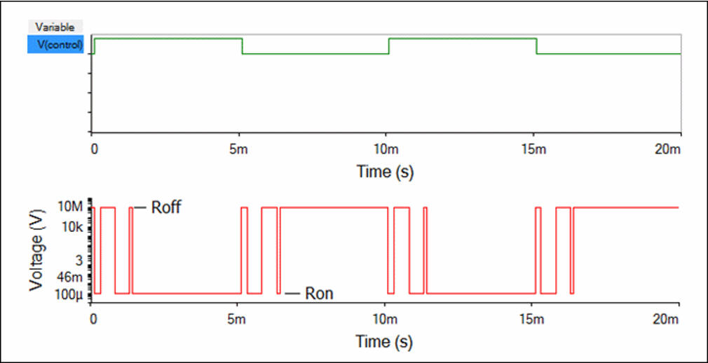
In Multisim Pro/Premium, you can simulate a real switch (so if you are using that software, you should actually show the bounce). It is called "Voltage Controlled SPDT Bounce". Since not many of you will try this, I show the trace here for a switch that is being turned on and off. The top trace is just indicating the intended ON state and OFF state, and the bootom is the resulting voltage as shown on an oscilloscope. Note the bounce betwen HI and LO before the switch settles on a value.

b) Wire the switch to the debouncing circuit discussed in class. Verify with the oscilloscope that the switch no longer bounces. If simulating, be sure to do this to show that the output still looks like you expect it should.
3. Synchronous Logic: the data (D) flip-flop uses a clock edge to trigger the input and send it to the output as described in class. Let's see this in action.
Note: If you are simulating parts 3 and 4, then do not bother with the debouncing circuit from 2b for those parts, just use the regular, already debounced, SPDT switch wherever it says to use the debounced switch.
Note: If you are simulating parts 3 and 4, and you only have Multisim Live Free (Basic) version, you do not have direct access to a D flip-flop. You can actually build one from NAND gates, but it is not ideally triggered on the rising edge of the clock signal. If you are using Pro/Premium, you have it no problem. Otherwise, please copy the D flip-flop from my account at https://www.multisim.com/content/dEsyq35sToc5eVKjAjqSwQ/lab-5-part-3/open.
a) Connect
the output from the debounced switch to the clock input of a 74175
D flip-flop (physical
chip); this will be the clock pulse on which the D flip-flop is triggered.
Connect a pushbutton switch to the D input (this is the "data" bit that is fed
into the circuit logic) and LEDs to the flip-flop's Q and notQ outputs (to show
whether the output is LO (0) or HI (1).
Verify that the flip-flop behaves as it is supposed to by creating a
truth-table, where one input is the D bit that you set as 0 or 1, and
the other input is the clock (the signal from the debounced switch), and the options are off (0), on (1),
and also rising edge (↑), and falling edge (↓).
4. Shift Register (serial to
parallel converter): The shift register remembers one bit, and passes that bit
along to the next flip-flop on each clock strike. Make the following connections to use the 4 D
flip-flops in the 74175 (physical chip) to create a 4-bit shift register. Or
in Multisim, duplicate your flip-flop until you have four of them, lined up
from left to right, and we will call them, from left to right D1, D2, D3, D4
as shown in class.
- Connect the debounced switch output to the clock input of the 74175, or to the clock input of each flip-flop.
- Connect the D1 input to a pushbutton switch (so that it can be high and low as input).
- Connect the Qi outputs to Di+1 inputs (for i=1,2,3). That is, connect each Q output to the next flip-flop D input.
- Connect the CLEAR (RESET) input to a pushbutton switch (again, setup so it can be high and low). Or in the simulation, just commect all the CLEAR/RESETS together, and to a single digital constant input.
- Connect LEDs to the Q1, Q2, Q3, Q4 outputs.
a) Set
the CLEAR input to 0 and observe the LED outputs. Now set the CLEAR input to a
1 and observe.
b) Set
the D1 input to 1 and activate/deactivate the debounced switch 5 times to
produce 5 clock pulses. Observe and discuss the resulting values on Q1, Q2, Q3, Q4 outputs
after each clock pulse.
d) Your four Q bits are a digital memory device. Assume they represent a 4-bit binary number, where Q4 is the 1's place, Q3 is the 2's place, etc. Clear the bits again, and now store the number 13 (in binary) in your 4 bit register. Describe how you did this and show a picture of the stored number.